 |
| March 06, 2012 | Volume 08 Issue 09 |
Designfax weekly eMagazine

Archives
Partners
Manufacturing Center
Product Spotlight
Modern Applications News
Metalworking Ideas For
Today's Job Shops
Tooling and Production
Strategies for large
metalworking plants
Engineer's Toolbox:
Latest optical micrometers measure surface defects on critical parts
The Depth Cam optical micrometer from Chadwick provides accurate measurement of surface defects.
By Jim McMahon
Whether it is scratches on a helicopter's rotor blades or on the fuselage skin of an aircraft, or corrosion pitting on industrial couplings, castings, transmissions, or engines, it is critical to evaluate the severity of mechanical damage to stress-bearing parts. These surface defects represent stress concentrations that are more susceptible to failure than the other areas of the component.
Very specific maximum allowances often apply to surface defects, which are essential to determine whether or not a part should be kept in service. To repair or replace the part can have significant structural and financial impact. For example, a helicopter's mast, which connects the chopper's motor to the main rotor, has a defect depth allowance of .012 in. to .015 in.
If the depth of the defect exceeds those parameters, then the part is at risk of breaking and must be replaced. But replacing such parts can be a very expensive proposition. In the case of helicopters, masts can cost as much as $25,000 to replace.
Careful visual inspection should, therefore, be standard protocol for any force-absorbing component that exhibits scratches, blemishes, or corrosion pits.
Hand-held optical micrometers
The portable optical micrometer has long been the tool of choice to measure the depth of these defects, from the surface to the bottom of the depression, thereby determining the severity of mechanical damage.
Optical micrometers are portable microscopes specifically designed for measuring depth. They are used for measuring three-dimensional relief along the z-axis within any x-y field of view, and they accomplish this by measuring the difference in depth between any two focal planes. The instrument is focused on a region of interest and set to zero. Then, as a second region is brought into focus, depth is shown on a digital display.
Optical micrometers serve as non-contact height gages and are ideal for small or intricate subject matter. This simple and practical capability has countless applications in almost every area of science, manufacturing, aerospace, quality control, and industry.
As an inspection tool, optical micrometers are simply outstanding, providing quick, accurate, and repeatable results where other methods are time consuming and inconclusive. Scratches, gouges, and corrosion pits are easily measured in instances where the fingernail test is often the only alternate method in use. If a component is scratched too deeply, time and money are saved by making quick and sure decisions, and even more money is saved by not scrapping parts that are well within tolerance. It is to everyone's advantage when the guesswork is removed from decisions regarding aircraft component integrity, for example.
From incoming raw materials to finished parts, optical micrometers routinely measure surface flaws, scratches, and corrosion. Both vendors and buyers improve their process controls by agreeing on what constitutes a reject versus an acceptable blemish whenever cosmetic value is a requirement.
Optical micrometers are particularly good for measuring the depth of corrosion pits, as built-in magnification makes it easy to find the deepest part within a given area. Hours of blend-out labor can be avoided when it is determined ahead of time that a corrosion pit is too deep.
These tools are also used to check dimensional accuracy, like calipers and other workshop and quality-control measuring equipment, in manufacturing and production environments. Serving as non-contact height gages, they can confirm the height of a component above a background or substrate on a micro-circuit or assembly; measure the depth of tiny steps, layers, and grooves; or the actual depth of small mold cavities, for example.
Introduced in the 1950s, optical micrometers hold several NSN's (National Stock Numbers); they are in the supply systems of several corporations and have been used on the space shuttle and the International Space Station.
Whether they are used to check dimensional accuracy or to measure the severity of flaws and defects, optical micrometers are compared to N.I.S.T. (National Institute of Standards and Technology) traceable standards and are required to be re-certified on a regular basis, just like other quality-control measuring equipment.
Optical micrometers get more mobile
There have been major product improvements and upgrades with portable micrometers over the years, but none that compare to the completely new and innovative designs of the latest models. The most prominent example is the newly re-designed portable optical micrometer by the J. Chadwick Company (Chadwick), who teamed up with Lincoln Laser Company (Lincoln) to collaborate on the design and manufacturing for a new-generation, electronic version of the portable micrometer. Chadwick is an OEM of portable optical micrometers, having manufactured analog and digital versions for the military and the aerospace industry since the early 1990s. Lincoln Laser specializes in the design, engineering, and manufacturing of high-precision mechanical, laser-based, and electro-optical systems.
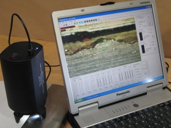
Chadwick's latest version, called the Depth Cam, was designed to handle resolutions as low as 1 micron and offers a number of electronic capabilities that have not been available in prior portable units. The intent was to build an instrument that was easier and faster to use, produced consistent detailed and accurate results, interfaced with a PC for real-time control and monitoring, and had the capability to store data for later evaluation and comparison.
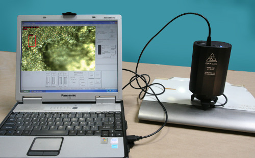
The Depth Cam with PC interface for real-time control and monitoring.
"Portable optical micrometers needed to bring a higher level of precision and integrity to this important judgment process," says John Chadwick, president of the J.Chadwick Company. "Should a defected part be repaired or replaced? An instrument that is giving inaccurate readings could cost a company many thousands of dollars in unnecessary new parts when the defective ones were still within compliance."
The first camera- and PC-based portable optical micrometer
Once the micrometer is positioned over a point of interest, the user does not look through a lens (as in prior portable micrometers), but instead controls the movement of the objective through a portable PC, by operating a mouse while viewing a monitor, or graphic user interface (GUI).
The optical micrometer has a microscope objective with a CCD array sensor positioned above it, having a resolution of 1,280 x 1,024 pixels. A light is shined at the surface of the part being viewed, and the array registers its position. The light is emitted from high-performance LEDs and channeled via fiber optics to the point of interest. The micrometer then will zero-out a linear scale, and the operator selects the bottom of the defect. The light is shined on that point of interest, and it is recorded on the CCD sensors.
The color USB 2.0 camera and illumination from the high-brightness LEDs are individually adjustable from a laptop. A 1-micron linear encoder provides high resolution, and a rechargeable lithium-polymer battery pack supplies power. A motorized focus is operated remotely from a laptop or by a rotary dial with five-way toggle on the instrument. Focus can run in velocity or position mode, and at different speeds and increments within each mode.
The system provides live image preview with real-time camera and focus controls, image capture, video, and zoom. Custom GUI buttons line the borders of the live image, and current depth value is always displayed and can be set or reset to zero at any position within the range of travel. Two region-of-interest boxes can be drawn via click and drag, for surface-A and surface-B selection, and focus metering optimizes focus within each region-of-interest box.
Images can also be archived for future reference. This allows comparisons to be made with prior measurements of the same part, or similar parts, to aid in evaluation.
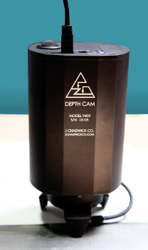
The Chadwick portable Depth Cam model 9400 can handle resolutions as low as 1 micron.
"Chadwick brought us in to take the hand-held optical micrometer to the next level, to make an electronic rather than a manual device," says Alex Biegel, mechanical engineer with Lincoln Laser. "We designed the electro-optics, software, and graphics for the unit. The engineering certainly had its challenges, designing the unit to have a scratch depth measuring capability to 20,000ths of an inch, and operating at the 1-micron level."
"The whole unit was modeled in 3D," continues Biegel. "That allowed us to figure out our three-dimensional packaging very accurately. We would also be manufacturing the instrument, so this ensured we would not encounter manufacturing problems later on down the line. It makes any updates, upgrades, and further engineering much easier."
Portable micrometers with 3D solid modeling on the horizon
In the near future, 3D solid modeling is possible. Multiple images from different focal planes will form a virtual solid that can be viewed from any angle by rotating with a mouse on screen.
Depth of field will be addressed by image fusion, where images from different focal planes can be combined into one all-in-focus picture, and video-text overlays will allow text, arrows, and calibrated scales to be drawn onto images.
Image analysis will also allow nodularity and porosity classification, plating thickness measurement, and grayscale thresholding.
Whatever tech improvements are on the horizon for portable optical micrometers, it is clear that the instrument has just recently taken a quantum leap forward in accuracy and user flexibility.
Want more information? Click below.
About the author
Jim McMahon writes on instrumentation and controls technology. His feature stories have appeared in hundreds of industrial and high-tech publications throughout the world and have been read by millions of readers. He can be reached at jim.mcmahon@zebracom.net.
Published March 2012
Rate this article
View our terms of use and privacy policy